Orla McCoy
Global Water Intelligence
Collaborators
Tags
Project NewsMarket TrendsYear in review: Fab investment in 2021
Below is a roundup of the main investment trends, including advanced packaging, public funding and more spending on DRAM equipment.
Share this insight
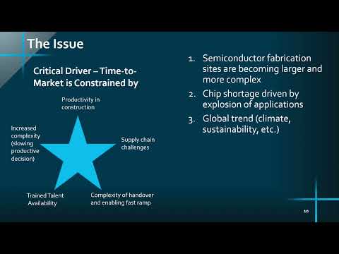
The past year saw investments aimed at expanding manufacturing at fabs to meet global demand for microchips. With total sales from semiconductor manufacturing equipment set to surpass $100 billion in 2021, investment well exceeded the previous industry record of $71 billion in 2020.
Advanced packaging drives fab expansion among heavyweights Demand for chips that optimise costs and power efficiencies is driving investment in 2.5D and 3D packaging. The Intel New Mexico fab began expansion in late 2021. The $3.5 billion expansion will include integration of Foveros – Intel’s breakthrough 3D packaging technology – and the resulting chips will service artificial intelligence and 5G applications. In December, Intel also announced an investment plan of $7 billion to expand manufacturing of advanced semiconductor packaging in Penang, Malaysia.
TSMC is installing equipment at its advanced packaging fab in late 2021, with production planned to start in 2022. The fab will utilise 2.5D packaging, a technology that is part of the company’s 3D Fabric brand.
Public support funds chip manufacturing
The past year has seen multiple national governments and city authorities announce support for chip manufacturing through publicly funded investments, tax incentives and other initiatives aimed at encouraging corporate investment. These moves have already resulted in plans for greenfield and brownfield fab projects, including infrastructure relating to water supply and wastewater treatment.
As one example, the South Korean government is looking to localise ultrapure water (UPW) production capabilities, with the goal of having 100% of UPW treatment plant design work and 60% of construction work performed locally by 2025. The scheme is just part of an overarching government plan to invest $430 billion in the domestic semiconductor industry through 2030.
Public investment in fab construction is also prevalent in other parts of Asia. The Japanese government, TSMC and Sony Semiconductor Solutions are collaborating on funding for a new $7 billion fab which will produce 28nm and 22nm chips by 2024. In China, state-owned Integrated Circuit Investment Industry Fund (CICIIF) announced US$531 million in spending to expand SMIC’s Shenzhen fab, bringing the project’s total investment to US$2.35 billion. The fab is expected to begin producing 300mm wafers in 2022 using 28nm technology nodes. SMIC is also expanding another 28nm process fab near Shanghai, with a portion of the $8.87 billion investment coming from the Shanghai Municipal People’s Government.
Meanwhile, local authorities in Texas are supporting semiconductor manufacturing through tax incentives. The city of Taylor will provide a 10-year, 92.5% rebate on property tax for Samsung Electronics’ $17 billion fab, which will manufacture advanced logic chips. In the city of Sherman, Texas Instruments will receive a 30-year, 90% tax abatement for four fabs together potentially worth $30 billion. Construction of the first and second fabs is to begin in 2022, with production expected as early as 2025.
EUVL drives 10nm nodes and smaller
Investment in smaller nodes continues to rise, which is evidenced TSMC announcing in March 2021 that $35 billion would go towards its new Arizona fab, which will include 5nm processing lines for 300mm wafers.
Intel announced their IDM 2.0 strategy, which involves greater development of the company’s 7nm technology, which requires use of extreme ultraviolet lithography (EUVL). The strategy also involves expanding use of third-party foundry capacity and building Intel Foundry Services, complimented by two new Arizona fabs - which will bring the Ocotillo campus’ total number of fabs to six featuring advanced technology Intel 20A, featuring RibbonFET and PowerVia transistor innovations, which are designed for manufacturing at smaller nodes. The former technology optimises power delivery, and the latter improves electrostatic control for more efficient power consumption. Intel’s Israel fab began a $10 billion expansion in 2021, which will contribute to the company’s 10nm and 7nm advanced node capacity. More to learn about the IDM 2.0 strategy is available through the recording of the Intel Keynote at UPM 2021.
According to SEMI, DRAM equipment represents the largest portion of equipment investment in 2021, rising to $15.1 billion, which is up 52% since 2020. The trend of increasing production of 10nm DRAM chips can be seen by the 2021 of SK Hynix’s new South Korean fab complex. These facilities will be the product of a $106 billion investment and rely on EUVL. The complex is expected to go live in 2025, making 10nm DRAM equipment for PCs, mobile devices, and servers. Nanya’s Taiwan fab will also deploy EUVL for manufacturing 10nm DRAM chips, as the company announced a $10.7 billion investment for adding 45,000 monthly wafer capacity.
Larger nodes endure the test of time
GlobalFoundries is distinguished by a strategy which avoids racing to ever-smaller nodes. Using 14nm technology and above, the company announced several major expansions in 2021, entailing investments worth $4 billion in Singapore and $1 billion each in Malta, New York and Germany. Though TSMC has secured 5nm technology and is rumoured to be piloting 3nm technology, the company is also putting additional capital towards larger nodes. In 2021, TSMC announced an expansion of its Nanjing fab to build capacity for 28nm nodes, which are expected to continue being key for mobile phone applications.
Larger-node chips have continued popularity among European manufacturers, as evidenced by Bosch’sopening of a fab in Dresden, Germany in June 2021. That project comprised a $1.2 billion investment in a facility with nodes up to 65nm. Additionally, STMicroelectronicsand Tower are collaborating on funding for a fab in Italy which will begin production in 2022. In the early stages of production, 130nm, 90nm and 65nm processes will be used.
Share this insight


Related resources
The Microelectronics Industry in 2023: A drive towards sustainability, reuse and growth in water-related spending