Alice Young
Global Water Intelligence
Collaborators
Tags
UPWGasesChemicalsSubstrate Environment Contamination Control – The Manufacturing Tools Perspective; A Summary
Share this insight
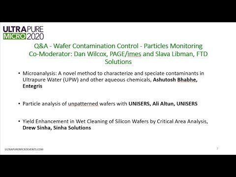
This webinar provided a deep dive into the effects and challenges of sub-10nm particles within the semiconductor manufacturing process. As we move towards 7nm and even 5nm device nodes, particle size becomes ever more critical, and so it is important to explore both the sources and solutions which will help improve device performance and yield.
Both Nabil Mistkawi, Samsung Austin Semiconductor, and Marcel Teunissen, ASML, provided detailed presentations which outlined the impact of particles on the wafer within different processes, summarizing the importance of contamination control and quality. As pointed out by Nabil, part of this is the selection of high-quality raw materials, such as UPW, liquid chemicals and gases. It is important to source these materials from trusted suppliers with strict protocols, who have a good understanding of material transportation and change points within the distribution network. As highlighted in a case study later in the webinar by Jim Snow, SCREEN SPE, 75% of particles within a wet processing tool perspective came from liquid contamination, highlighting not only the need for high purity materials, but also better filters and components.
As pointed out by Abbas Rastegar, Applied Materials, one of the key challenges, and also opportunities within contamination control, is the need for better particle metrology. Whilst there are ways to approximate down to critical particle size, direct particle detection has been a challenge for a number of years. The development of capable particle metrology will be an important driving factor for increasing yield, improving device performance, and future technology development.
Rushi Matkar, Intel, provided an enduser perspective towards this challenge, stating that it is a combinatorial problem between patterning process systematics and random defects. There was a clearer delineation in the past, but as process technology becomes tighter, this distinction becomes more muddled, and it becomes harder to debug the problem. Rushi’s message to everyone is to get innovative! This is not only a filtration problem, but also a purification problem. Technology and computing are integral to daily life, and so the industry needs to keep pushing forward to overcome such challenges.
If you’d like to hear the full discussion around proactive quality management and substrate environment contamination control, please visit the webinars page, where you can watch a full webinar recording. With thanks to Dan Wilcox, Page/imes, Nabil Mistkawi, Samsung Austin Semiconductor, Marcel Teunissen, ASML, Jim Snow, SCREEN SPE, Abbas Rastegar, Applied Materials, Rushi Matkar, Intel, and Slava Libman, FTD Solutions, for their time and contributions to this webinar.
Share this insight
Related insights
5 key UPMU workshop takeaways: UPW system design principles

Georgia Bottomley
Global Water Intelligence
Expert Q&A – Driving Yield and Reliability Solutions in the Semiconductor Industry

Orla McCoy
Global Water Intelligence
News-in-brief: June 2023
Orla McCoy
Global Water Intelligence
Related resources
Substrate Environment Contamination Control - The Manufacturing Tools Perspective
Ozonated Water Reclaim on SCREEN Wet Tools
Eco-efficiency in ultrapure water treatment system design and operation