Orla McCoy
Global Water Intelligence
Collaborators
Tags
Energy ConservationWater ConservationSustainability5 trends from the UPM 2023 Environmental Sustainability Panel
Read the summary and watch the recording now.
Share this insight
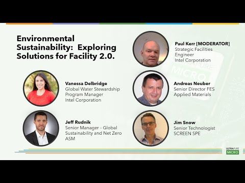
At the UPM 2023 Conference, the Environmental Sustainability Opening Panel presented actionable insights and opportunities for the entire semiconductor value chain. The panel included representatives from across the supply chain – including a fab engineer, a tool provider, a technology provider, and an engineering consultant – and each provided their perspective.
Below is a summary of five things we learned from this panel, with insights from:
- Nabil Mistkawi, Principal Technologist/Engineer at
- Jim Snow, Senior Technologist,
- Walt Kozlowski, Senior Director of Client Sustainability Solutions, Xylem
- Rob Simm, Senior Vice President, Stantec
- Alan Knapp, Senior Director – Microelectronics, Xylem
In addition to the summary, you can watch the recording and view the slides on the UPM Technical Knowledge Base.
1. As the industry approaches extreme scaling, fabs are demanding solutions to mitigate the environmental impact of advanced chip production.
As the semiconductor industry pursues chips for advanced computing, artificial intelligence, and other advanced applications, the environmental impact of producing a single microchip soars. Alan Knapp, Senior Director – Microelectronics at Xylem noted that the production of chips at the legacy process node of 90nm requires about 300 process steps. Now, modern chips manufactured at the smallest nodes require up to 1100 process steps. This extreme industry shift has led to increased usage of chemicals, gases, and space.
Jim Snow, Senior Technologist at SCREEN, presented Figure 1 at UPM 2023, which was taken from a 2022 study performed by Imec into the relationship between scaling and ultrapure water (UPW) usage, energy usage, and carbon dioxide emissions. Snow also noted that chip production at the 28nm technology node requires nearly 6 liters of water per square centimeter of wafer, but in the nanosheet levels, this figure rises to over 14 liters. As such, when producing chips at the smallest technology nodes, each 300mm wafer can require about 10,000 liters of water.
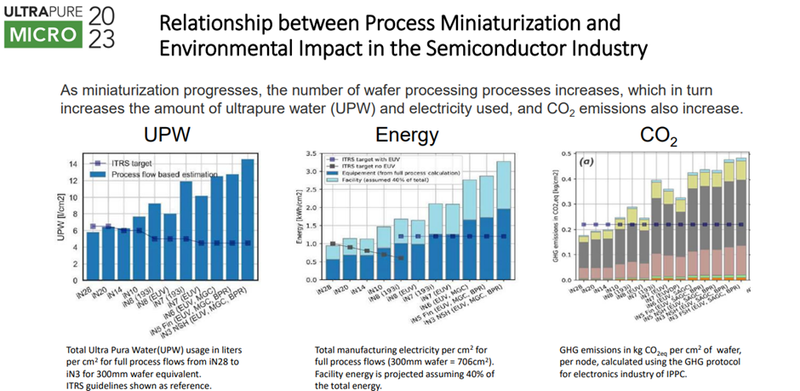
Figure 1. Source: SCREEN, UPM 2023, taken from Imec
2. Innovation in the process chemistries is shifting towards sustainability.
Nabil Mistkawi, Principal Technologist/Engineer at Samsung Austin Semiconductor highlighted that the industry recognizes the impact of scaling on resource intensity, and innovation can change the long-standing chemistries used in fab processes. The efforts lie especially in trying to develop less chemically harmful formulations and trying to reduce the amount of time needed per process step. For example, Mistkawi explained that at Samsung Austin Semiconductor, a newly invented chemical replaced a harmful solvent which had been causing difficulties with disposal. In addition, this new chemical reduced the time spent processing the wafer at this particular step to 2 minutes, rather than the previous time of 2 hours.
3. Sustainability is increasingly in-built for process tools
Segregation and recycling at the tool represent some of the most significant opportunities for minimizing water and chemical usage, especially as 75% of water in a semiconductor fab is used in the manufacturing process – primarily in chemical mechanical planarization (CMP) and wet etch. The onset of single-wafer processing tools for wet processes signifies an opportunity for improved waste stream segregation by adjusting the wafer's position relevant to drain cups. Further downstream, valves can be employed to isolate different drain lines, making it easier to manage waste streams. Snow highlighted that, for some facilities which have adopted these solutions, it has improved the waste disposal options for certain contaminants of concern for discharge limits, such as tetramethylammonium (TMAH) and N-Methyl-2-pyrrolidone (NMP).
Additionally, the semiconductor industry is exploring the recycling of chemicals at the tool level. Sulfuric acid represents a significant acid load in facilities. The treatment of waste streams and brine management is a substantial challenge, with considerations for disposal costs and shipment logistics. Since most of the sulfuric acid waste from the photoresist stripping process is relatively clean, there is an opportunity to segregate and recycle a large volume of sulfuric acid back into the process.
4. The execution of sustainability goals requires facilities engineers to prioritize carefully.
Whilst sustainability is becoming increasingly critical to corporate intentions, the reality is that facilities need to make carefully informed decisions about the trade-off between sustainability and cost. Furthermore, choosing the option which has the biggest impact in terms of sustainability can bring more difficult engineering solutions in future years.
Walt Kozlowski, Senior Director of Client Sustainability Solutions at Xylem highlighted that in Figure 2 the sustainability impact of end-of-pipe wastewater use is extremely high, and there are other engineering benefits as it is a single system with easier maintenance and monitoring requirements. However, it can be costly in terms of piping, pumping, and footprint. Future expansion or the implementation of new technologies at a later stage also becomes more difficult with end-of-pipe reuse. Kozlowski urged the audience at UPM not to forget that easier sustainability wins still have measurable impacts for facilities, and highlights examples such as rainwater reuse or the increasing the cycles of concentration on a boiler, among other options.
Kozlowski also highlighted that Minimum Liquid Discharge (MLD) contributes significantly to sustainability programs without the heavy trade-offs relating to energy and expenditure which engineers experienced whilst implementing Zero Liquid Discharge (ZLD).
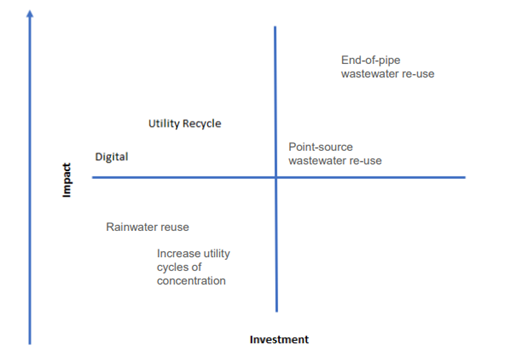
Figure 2. Source: UPM 2023, taken from Xylem
One of the biggest opportunities for the future for water in the semiconductor industry will be recycling into UPW systems.
Despite the panel’s emphasis on easy sustainability wins, it is still important to look to the future and understand how the resilience of the water supply to the fabs, and difficult decisions which facilities will face.
Rob Simm, Senior Vice President at Stantec, highlighted that sustainability goals will eventually compel facilities to adopt more recycling of water for makeup into the UPW system, as corporate ambitions – such as those held by Samsung – call for no rise in water usage despite increases in production capacity. Simm explained that recycling into UPW systems is being done is some fabs, but generally there is a concern amongst the process engineers in the fab that the water will be contaminated and affect yield. Generally, it is not the technical feasibility of using reclaimed water for UPW makeup which presents a problem but the need from fab engineers to understand data from analytical technologies so that the risk can be weighed up.
For further information on this panel watch the recording and view the slides on the UPM Technical Knowledge Base.
Share this insight
Related insights
Q&A Results with ElectraMet: Copper recovery from CuCMP Wastewater

Cameron Lippert
Electramet
The Rising Tide of CEDI: Why it is Outshining Traditional Ion Exchange in High-Purity Applications (Part 2)

Orla McCoy
Global Water Intelligence
The Rising Tide of CEDI: Why it is Outshining Traditional Ion Exchange in High-Purity Applications (Part 1)
Orla McCoy
Global Water Intelligence
Related resources
Environmental Sustainability - Opening Panel
Environmental Sustainability: Exploring Solutions for Facility 2.0